Buried Via PCB
PCBA is a process requiring knowledge covering PCB manufacturing assembly, PCB design, fabrication and a strong understanding of the final product. ZF is a professional pcb manufacturing companies with high-quality, all of our products have obtained ISO9001, ISO13485: 2016, IATF16949: 2016, IPC-A-610E, UL, RoHS certifications.
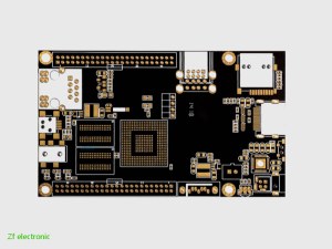
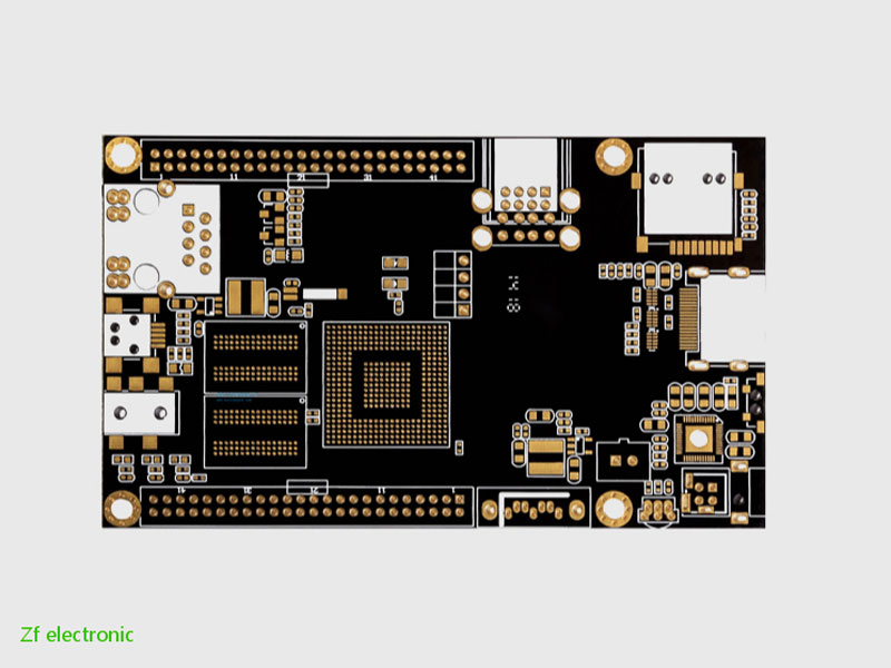
A buried via is a connection of any circuit layer inside the PCB but not connected to the outer layer. The via cannot be drilled after bonding because it must be drilled on the individual circuit layers first. After partially bonding the inner layer, it has to be plated before finishing the bonding, which is more laborious and therefore more expensive than the original through via and blind via. Usually, it is only used in high-density(HDI) PCB to increase the available space for other circuit layers.
1. What is via?
The via is an important factor in the design of multi-layer PCB and consists of three main parts, including drill hole, the pad around the hole and the POWER layer. When talking about its process, it should be firstly plated a layer of metal by chemical deposition on the cylindrical surface of the via wall to connect the copper foils that need to be connected to the middle layers. The upper and lower sides of the via will be made into a common pad shape, which can be directly connected with the lines near the two sides or not.
2. Classification of vias by function
In terms of function, vias can be divided into two categories. One is used for electrical connection between layers while the other is used for fixing or positioning devices. As for the process, the vias can be generally divided into blind via, buried via and through via.
(1) Blind via
Blind via hole is located on the top and bottom surfaces of the PCB with a certain depth. It is used to connect the line on the surface and the underlying inner line and its depth usually does not exceed a certain ratio (aperture).
(2) Buried via
It refers to the connection via that is in the inner layer of buried via PCB which will not extend to the surface of the circuit board.
Both of above-mentioned two types of vias are located in the inner layers of the circuit board, which are completed by using a through-via forming process before lamination. There may also be several inner layers overlapping during the via formation process.
(3) Through via
The through hole vias penetrate the entire circuit board and can be used for internal interconnection or as a positioning via of component installation. Because of its easier implementation and lower cost in the process, most of the PCBs use it instead of the other two kinds of vias.
The advantages of the blind via and buried via
In the non-through-via technology, the application of blind via and buried via can greatly reduce the size and weight, as well as the number of layers and costs in printing circuit boards, moreover, improve the electromagnetic compatibility, increase the characteristics of electronic products, making the design simpler and faster.
As for the traditional PCB design and processing, there are many problems brought by through vias. First of all, through-vias occupy a large amount of effective space. Secondly, a lot of through-vias densely packed in one place also make the wiring of the inner layers in the multilayer PCB difficult. That is because they will take up the space required for alignment, destroy the impedance characteristics of the power supply and make the power ground plane ineffective. What's worse, the conventional mechanical method of drilling will be 20 times the workload of non-through hole technology.
If you have questions about our buried via PCB production capacity, or the specifications required for your custom project are not listed on this page, please feel free to contact us. We will reply within one workday. We will continue to provide quotation support and design support. Welcome to learn about our production process.
Personne à contacter : He Mike, +86 188 7956 1688
Bonne affaire : acheter au vendeur
Nous vous invitons à lire nos conditions générales d'utilisations. Vous pouvez aussi vous rendre sur nos FAQ et consulter notre page d'informations sur les risques liés à la contrefaçon.
|
Cette page concerne les importateurs et exportateurs de Buried Via PCB Rechercher dans la catégorie : Véhicule Rechercher dans la catégorie : buried |
Dimanche 22 septembre 2013
Quantité : 40 TN/ MOI - Prix : entre 3,50€ et 4,50€
STEAK HACHE X gr. HALAL GLUTEN produit congelé IDENTIFICATION DU PRODUIT Code produit 03080 / I Nom Hamburger STEAK HACHE origine Espagne CARACTERISTIQUES DU PRODUIT Dimension / Poids 101mm x 9,5 mm, 80 gr Boeuf Ingrédients 100% CONSERVATION 12 mois La température de...
halalastur
- 33420 - Lugones
- +34 6 30 00 57 64
Dimanche 10 août 2014
Quantité : as you nee - Prix : USD 3500-88888
Quick details: brand : Yong hua model; YHQ 360 Reducer: ZQ350 Ratio: 1: 31.5 roller size: 360*250 capacity: 0.1-3t/h oval size: 2.26*1.53*1.76 Spindle speed : 13-15r/min function: by pressing , the machine can mold a variety of mineral powder,metal powder, coal powder,coke...
Henan Zhengzhou Yonghua Machinery
- olina1
- 450000 - zhengzhou CITY
- +13 6 07 69 93 63
Mardi 20 mai 2014
Quantité : 1000 - Prix : N/A
TV150A VGA KVM Chainable Extender over IP with Audio is the innovative solution applied for a wide variety of HID devices extending in terms of excellent compatibility of “True USB emulation” technique, even supports the latest 10- point touch screen, and signals extended...
ACAFA Information Co.
- epanio
- 335 - Dasi Township
- +88 6 33 07 13 00


