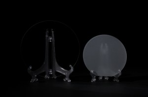
STANDARD SAPPHIRE WAFERS (C-PLANE)
CRYSCORE can offer Epi-Ready grade optical sapphire wafer with a very low surface roughness in complete orientation options.
C plane sapphire wafers are being extensively used for epitaxial growth of III-V and II-VI compounds, such as gallium nitride (GaN), aluminum nitride (AlN), for bright blue and green LED and laser diodes.
Different Sizes of Standard Sapphire Wafers
1 Inch C-plane(0001) Sapphire Wafers
After over 12 years extensive experience, CRYSCORE can produce high quality sapphire wafers in all orientations with unpolished and polished sides.
2 Inch C-plane(0001) Sapphire Wafers
CRYSCORE polishes the sapphire wafers by special CMP (Chemical Mechanical Polishing) technology, which is a widely used planarization technology.
3 Inch C Plane Sapphire Wafers
Sapphire is an important material used widely in the growth of III-nitride epitaxial layers (GaN, AlN, InN, AlGaN, InGaN, InAlN, etc.)
4 Inch C-plane(0001) Sapphire Wafers
Sapphire wafer is being used extensively as a substrate for III-V nitrides and for many other epitaxial films.
5 Inch C-plane(0001) Sapphire Wafers
5-inch C-plane (0001) sapphire wafers are not as common as other specifications. However, its quality manufactured by CRYSCORE is as good as gold.
6 Inch C-plane(0001) Sapphire Wafers
Based on the continuous upgrade of sapphire technology and the rapid expansion of the application market, 4 inch and 6 inch substrate wafers will be more adopted by mainstream chip companies.
8 Inch C-plane(0001) Sapphire Wafers
The 8-inch sapphire wafers can enable chip maker to roll out more productivity, which will help them drive down costs dramatically.
Technical Applications of Standard Sapphire Wafers
C-plane sapphire wafers and c plane sapphire substrate are widely used to grow III-V and II-VI deposited films of wide band-gap nitride and oxide semiconductor materials such as gallium nitride (GaN), aluminum nitride (AlN), indium nitride (InN), zinc oxide (ZnO ultraviolet light emission) and tin oxide (SnO2 ultraviolet luminescent material), etc.
In addition, standard C-plane(0001) sapphire wafers are widely applied to fabricate LED white and blue light, ultraviolet and deep UV LED epitaxial wafers by Metal-Organic Vapor Deposition(MOCVD), Molecular Beam Epitaxy (MBE), Plasma Enhanced Chemical Vapor Deposition(PECVD) and other epitaxy growth methods.
CRYSCORE standard sapphire wafers also are used as the substrates of heterojunction bipolar transistor (HBT), a laser diode (LD), UV detector, nanotube, and the heat dissipation material of high temperature and high power high-frequency electronic device.
Competitive Advantages of CRYSCORE's Sapphire Wafers
99.999 % high purity single crystal Al2O3 substrate material.
Special CMP (Chemical Mechanical Polishing) technology to ensure its performance at a low cost.
Excellent surface quality in all orientations (less than 0.2 nm for C-plane, less than 0.5 nm for A-plane, M-plane, R-plane, N-plane, V-plane, 10-14, etc.)
Cleaned in class 100 cleanroom by ultrapure water with quality above 18MΩ *cm.
25 pcs a pack or single pack is available to maximize customer flexibility in their research.
Traceable product serial number.
Compact carton packaging for safer shipping and cost-saving.
Standard wafers are Generally in stock to ensure a quick delivery.
As a professional sapphire wafer supplier, CRYSCORE aims to provide customers with the best products and services, and let our technology benefits the world.
Localisation : No. 49, Jiefang East Road, Shanyang District, JIAOZUO 454000, HENAN, CHINA, 454000 Jiaozuo,
Personne à contacter : Zhu Wind, +86 0391 393 3936


