 |
|
|
Divers
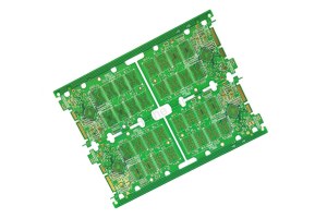
Heavy Copper PCB
|
|
Cette page concerne les importateurs et exportateurs de Heavy Copper PCB Rechercher dans la catégorie : Divers Rechercher dans la catégorie : copper, heavy |
Saturday 20 February 2016
Quantité : 1000 MT PE - Prix : 300/mt CIF
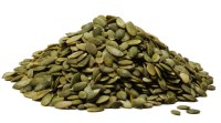
PUMPKIN SEEDS GROWN WITHOUT SHELL NEW CROP 2015 TOP GRADE AND COMPETITIVE PRICE PRODUCT DETAILS AND SPECIFICATIONS Product name Dark Green Pumpkin Seeds Year of production Crop 2016 Origin Thailand Grade A,AA grade Style Common or Organic Moisture 9%max Purity 99...
Khun Jack Partnership Ltd
- 5000 - Chaing Mai
- +66 9 68 75 20 43
Tuesday 06 January 2026
Quantité : 108
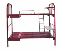
Product Details Bed Type : Panel Layer : 2 layers Frame Material : Metal Color : Pink, Blue, Cream white, Browm… Headboard Included: Yes Under bed Storage : No Product Care : Wipe with a clean, damp cloth Painted frame · One set include - Headboard. - Footboard. - Two...
Qui Phuc Company Limited
- Luck06
- 700000 - Ho Chi Minh
- +84 9 86 58 28 62
Friday 21 June 2013
Quantité : 2000T/mont - Prix : 880usd
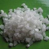
99.5% high purity white fused alumina/WFA 3-5mm Description: White fused alumina oxide powder is a high-quality raw material, made of fused refin ing crystal, high purity, self-sharpening, good acid and alkali resistance, high temperature, thermal properties and stability it...
Henan Sicheng Co, ltd
- 450006 - Henan province
- 0086 371 68706009
- 8615890630517


