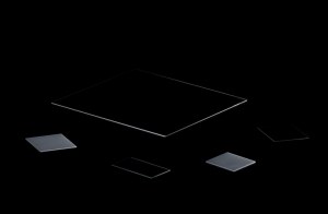
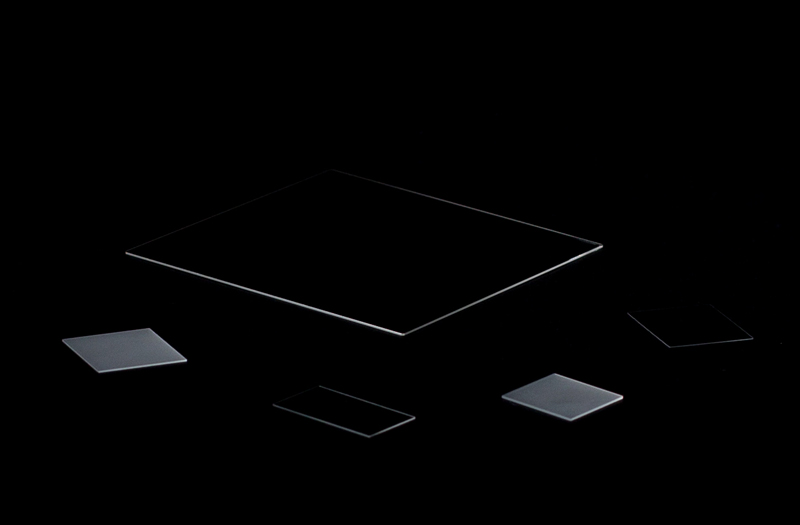
As a professional sapphire wafer manufacturer, CRYSCORE can provide standard or optical sapphire wafers with any orientation applied to epitaxy, as well as sapphire windows with any specifications applied to optics. Patterned sapphire substrates and sapphire ingots also can be provided. Expert in sapphire optics manufacturing.
SILICON ON SAPPHIRE
A Brief Introduction of Silicon on Sapphire Technology
Silicon on sapphire (SOS) technology is a hetero-epitaxial process for metal-oxide-semiconductor (MOS) integrated circuit (IC) manufacturing that consists of a thin layer (typically thinner than 0.6 µm) of silicon grown on a SOS wafer (Al2O3). SOS wafers are part of the silicon-on-insulator (SOI) family of CMOS (complementary MOS) technologies. Typically, high-purity artificially grown sapphire crystals are used.
The silicon is usually deposited by the decomposition of silane gas (SiH4) on heated sapphire substrates. The advantage of sapphire is that it is an excellent electrical insulator, preventing stray currents caused by radiation from spreading to nearby circuit elements. SOS faced early challenges in commercial manufacturing because of difficulties in fabricating the very small transistors used in modern high-density applications.
This is because the SOS process results in the formation of dislocations, twinning and stacking faults from crystal lattice disparities between the sapphire and silicon. Additionally, there is some aluminum, a p-type dopant, contamination from the substrate in the silicon closest to the interface.
Silicon on Sapphire Technology
Why is Silicon on Sapphire Technology So Important to Integrated Circuit
Due to sapphire has high permittivity that can eliminate the interaction between components of the integrated circuit, not only can reduce leakage current and parasitic capacitance, enhance radiation resistance and reduce power consumption but also can improve the level of integration and two-layer wiring, thus, sapphire is the ideal material for large scale and very large scale integrated circuit.
Silicon on sapphire technology provides ideal isolation and reduces the parasitic capacitance at the bottom of the PN junction, so it is suitable for high-speed large scale integrated circuits to achieve high speed and low power consumption. This process is generally used to make CMOS circuits.
In addition, in the SOS microelectronic circuit design and production, all kinds of semiconductor devices usually need to make on the structural integrity silicon thin film, and because thermal expansion coefficient of silicon is similar to sapphire, a silicon monocrystalline film (100) can be grown on the surface orientation(1-102) of the sapphire substrate by heteroepitaxy.
At present, sapphire crystal has become a widely used substrate for the growth of semiconductor materials.
Localisation : No. 49, Jiefang East Road, Shanyang District, JIAOZUO 454000, HENAN, CHINA, 454000 Jiaozuo,
Personne à contacter : Zhu Wind, +86 0391 393 3936


