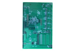
Lead-free HASL is to coat a layer of tin-lead alloy on the copper surface to prevent the oxidation of the copper surface and provide a good welding base for the subsequent assembly process. What is hot air leveling? It is actually a process of combining dip soldering and hot air leveling, and coating eutectic solder in the metalized holes of lead-free printed circuit boards and printed wires. The process is to first dip the lead-free printed circuit board with flux, then dip the molten solder, and finally pass between the two air knives. Use the hot compressed air in the air knife to remove the excess on the printed board The solder is blown off, and at the same time, the excess solder in the metal holes is eliminated, thereby obtaining a bright, smooth, and uniform solder coating.
Features of Lead Free HASL PCB
The immersion tin pcb process can form a flat copper-tin intermetallic compound. This feature makes the immersion tin have the same good solderability as hot air leveling without the troublesome flatness problems of hot air leveling; nor does it have electroless nickel plating / Diffusion issues between gold and metal; just the tin immersion board cannot be stored for too long.
Immersion tin does not bring any new elements into the solder joint, which is especially suitable for communication backplanes. The use of the immersion tin board is restricted due to the inconvenience of storage and the carcinogens contained in the process. About 5% -10% of PCBs currently use a dip tin process.
Parameters of Lead Free HASL PCB
1. Prevent oxidation of bare copper surface; 2. Maintain solderability
SPEEDAPCB has a mature HASL production line, as well as particularly experienced engineers, we will do our best to provide you with the perfect plate making service.
Characteristics of Lead Free HASL PCB
- The most prominent advantage of solder coating with hot air leveling is that the coating composition always remains the same, and the edges of the printed circuit can be completely protected.
- The cost of hot air leveling is lower than other surface treatments, the process is mature, and the weldability is good.
Advantages and Disadvantages of Lead Free HASL PCB
Advantages
-Tin-lead solder is not used.
-Excellent weldability.
-Lower price.
-Allows large processing Windows
Disadvantages
-Not suitable for smaller components.
-High processing temperature.
-The difference of thickness between big bonding pad and small bonding pad.
Difference between Lead Free HASL PCB and HASL PCB
1.From the surface, lead free hasl pcb is duller, but hasl pcb is brighter. The lead free hasl pcb wettability is a little worse than hasl pcb.
2.Lead in hasl pcb is harmful to human body, and lead free hasl pcb is not.
3.The lead content of lead free hasl pcb does not exceed 0.5. Hasl pcb can reach 37.
4.Hasl pcb will improve the activity of the tin wire in the welding process. Leaded tin wire is relatively better than lead free hasl pcb.
Performance Difference of HASL PCB and Lead Free HASL PCB
If the melting point of lead is about 183 degrees, then the temperature of the tin spraying furnace needs to be controlled at 245 degrees to 260 degrees, and the over-peak temperature needs to be controlled at 250 degrees, and the reflow temperature at 245 to 255 degrees. The lead-free melting point of about 218 degrees, then the spray tin furnace temperature needs to be controlled at 280 degrees to 300 degrees, over the peak temperature needs to be controlled at 260 degrees, reflow temperature at 260 to 270 degrees. Lead will increase the activity of tin in the soldering process. Leaded tin wire, in contrast to the case of lead-free tin wire to use, and lead-free spray tin than lead spray tin melting point is high, the welding point will be much stronger.
Localisation : 4F,wangdefu Building,Wanjiali Road,Furong District,Changsha,Hunan, 427000 Changsha,
Personne à contacter : Molly Tu speedapcb, +86 0731 15387574935


