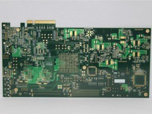
Among the large-scale use of PCI and optical modules and cable sockets, the goldfingers PCB has been divided into: long and short gold fingers, broken gold fingers, split gold fingers, gold finger plates in the process of processing, need to pull gold-plated wire, conventional gold finger processing is relatively simple, the length of the pcb finger connector requires strict control of the gold finger lead and requires a second etching to complete. Broken golden finger connector PCB than length The difficulty of the gold finger is increased, and the dry film is required to be processed three times. The lead does not need to be left for 4 times to complete the production of the gold finger .90% of companies are unable to process the control of the golden finger. PCBSky processing plug gold fingers PCB and long and short gold fingers PCB, broken section Gold finger PCB, master the core manufacturing technology, single gold finger gold plating thickness up to 50U gold thick, industrial graphics card PCI can be processed to 50U gold thickness.
The most common PCB gold fingers design appears on the graphics card and memory stick inside the computer.
Why Choose circuit board fingers?
★ A unique role of PCBA needs to be interconnected with the motherboard but needs to be replaced easily. Design the golden finger and slot connection, similar to the relationship between the power plug and the socket.
★ Because gold has good conductivity and inertness, it ensures the conductive effect without oxidation, and it also ensures sufficient conductivity after frequent insertion and removal of gold.
Gold Finger Definition and Role
Gold Finger: (Gold Finger Connector or Edge Finger Connector) Insert one end of the PCB into the connector card slot, and use the connector pin as the external connection of the pcb board to make the pad or copper contact with the corresponding pin. To achieve the purpose of conduction, and plated nickel or gold on this pad or copper plate of pcb board, because it is a finger shape, it is called gold finger. The reason why gold is chosen is because of its superior conductivity and oxidation resistance. . But because the cost of gold is extremely high, it is only used for local gold plating such as gold fingers.
Gold Finger PCB Design Considerations
1. First ensure that the length, width, position and card slot of the gold finger are fully matched to ensure proper interconnection.
2. The foolproof KEY SLOT designed on the PCB board, the width, height, position and the convexity in the card slot are completely matched.
3. Part of the PCB needs a shorter design of individual fingers, if you can not directly add a wire under the finger, you need to consider how to conduct electricity during pcb gold plating.
4. The angle and depth of the beveled edge of the gold finger are the same as the length of the finger. Do not cause the finger to be short or the beveled edge after the beveled edge.
Welcome to custom Low Cost PCB Fabrication - Gold Fingers PCB from Shenzhen PCB Manufacturer. And welcome to custom pcb fabrication from PCB MANUFACTURER CHINA.
Localisation : Building 1, Huaide Cuigang Industrial Zone 3, Fuyong Street, Baoan District , Shenzhen, Guangdong 518103, China , 518103 Fuyong Street,
Personne à contacter : Mo Jack, +15 9 76 88 36 32


